
Intel will start making 10nm chips this year it claims will lead the industry in transistor density using a metric it challenged rivals to adopt. Separately, it announced a 22nm low-power FinFET node to compete for foundry business with fully depleted silicon-on-insulator (FD-SOI) from rivals such as Globalfoundries.
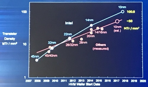
At 10nm, Intel will pack 100.8 million transistors per square millimeter. It estimated 10nm foundry processes now in production from TSMC and Samsung have about half that density.
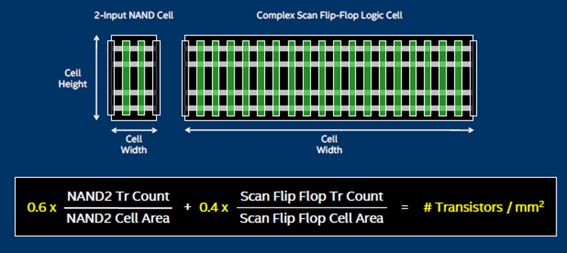
Intel’s metric averages density of a small and a large logic cell. Specifically, it uses a two-input NAND cell with two active gates and a scan flip-flop cell with as many as 25 active gates.
“I think it’s a comprehensive, quantitative and honest metric,” said Mark Bohr, a senior fellow and director of process architecture and integration. “TSMC and, I think, Samsung used to quote it, but my guess is they weren’t looking very good with this metric anymore,” he said.
The existing metric of multiplying gate pitch and cell height gives a relative advance between nodes, rather than an absolute number of a node’s capability. In addition, it does not include a variety of factors embraced by the density metric Intel proposed, Bohr added.
Whatever the metrics, Intel said it will start making 10nm Cannonlake chips in the second half of this year, three years after it launched its 14nm process. It expects to continue a three-year cadence, stretching 10nm with two annual upgrades to be called 10+ and 10++.
“Even with the longer time between nodes, we’re staying on the same cost per transistor curve and we expect this will continue through the 10nm generation,” said Stacy Smith, executive vice president of Intel’s fab and sales groups.
Interestingly, Intel’s 14++ sports higher performance than its initial 10nm process. However the 10nm node delivers lower power and higher density.
Intel gave more details than usual about its 10nm node. The x86 giant needed to be more forthcoming to show its advantages over 10nm processes already in production at foundry rivals TSMC and Samsung.
Specifically, Intel’s10nm node sports:
34nm fin pitches
53nm fin heights
36nm minimum metal pitches
272nm cell heights
54nm gate pitches
Intel claimed the node sports the tightest gate and metal pitches in the industry and marks the industry’s first use of self-align quad patterning. FinFETs are 25 percent taller and more closely packed than on its 14nm node.
The company described two transistor innovations to compensate for the rising costs of more lithography patterning steps. A contact-over-active-gate (COAG) helps deliver an additional 10 percent density; a single rather than double dummy gate at 10nm provides additional scaling advantages.
Next page: Praise for 10nm, mixed reactions for metric
Intel claimed its 10nm process is twice as dense as rival nodes. (Images: Intel)
----Form EE Times