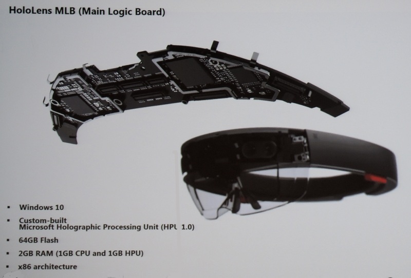
BRUSSELS – Microsoft gave a look inside its HoloLens and the Holographic Processing Unit that drives it at the Imec Technology Forum here. The HPU is among an emerging class of specialty accelerators.
In late March, Microsoft started shipping a developer’s version of HoloLens, its novel augmented reality goggles. The release generated a flood of teardowns but until now they lacked commentary from the headset’s designer.
“We have showed HoloLens for last 18 months, focusing usually on the experience and the software -- this is the first time we will talk about the hardware,” said Ilan Spillinger, corporate vice president of HoloLens and silicon at Microsoft.
The HPU at the core of the headset is essentially a data fusion sensor. It takes inputs from an array of sensors on the HoloLens include four environmental sensors, a miniaturized Kinect depth camera and an inertia measurement unit. It accelerates algorithms that track the user’s environment, movements and gestures and displays holographic images.
The 28nm HPU is essentially a highly customized DSP array running at less than 10W max. It includes an unknown number of Tensilica DSP cores optimized to run hundreds of HoloLens-specific instructions.
Each core is customized for a particular function and subset of instructions. In what sounds like a non Von Neumann architecture, each typically has its own unique organization of related memory units.
It accelerates “new style algorithms that need special local memories and a unique memory architecture, not a typical level 1-2-3 cache,” he said.

The HoloLens HPU rides a sleek motherboard tailored to fit the headset. (Images: EE Times)
Click here for larger image
The headset is powered by a 14nm Intel Cherry Trail SoC with embedded graphics running Windows 10. The two-sided motherboard also contains 64 Gbytes flash storage and 2 Gbytes external memory split evenly between the HPU and Cherry Trail SoCs.
Spillinger would not comment on the road map for the HPU except to say he “sees opportunity for running algorithms we didn’t think about.”
The HPU fits roughly in the category of a new accelerator Googleannounced last week for its data centers as well as one in the works at a startup.
Spillinger called on semiconductor engineers to pave a road to higher performance, lower power chips to help him build lighter, cheaper headsets packing more sensors and features.
The HoloLens chief started his career at Intel working on Centrino, its first dedicated notebook processors. Later, he moved to IBM designing Infiniband and Power chips and later helping Microsoft and Nintendo develop ASICs for the Xbox 360 and Wii consoles.
In late 2007, Spillinger joined Microsoft and started work on the Kinect. The project later merged with efforts by other engineers to develop an augmented reality headset and the HoloLens project was born.
----Form EE Times